MAXIS Engineering Inc.
We can offer solutions that enable high quality production in the BGA/CSP manufacturing process.
Solder Bump Flattening Technology by MAXIS-ENGINEERING INC.

About Bump Flattening
・Pressing the top of solder bump which constructed in semiconductor.
substrate boards, and make the top of solder bump flat.
The reason why solder bump needs to be flat
- In case of connecting solder bump of BGA/CSP boards in SMT and FC connect, every bump has to be connected with both passive electrode terminal at one time. With the view of reliability improvement of connecting, the height of solder bump needs uniformity and flatness.
- In case of mounting flip tip, it may cause mount slip when both faces of bump are spherical surface. To prevent from mount slopping, it is effective to make one side of bump flat.
- Bump flattening enables improvement of flux stability and improvement of connectivity.
Bump Flattening press causes the breakage of hard oxidation film in bump surface. It is effective to improve the connectivity.


Flattening Punch
The features which are demanded for flattening punch
-
High heat conductivity
-
High hardness
-
Low heat deformation
Above features has to be integrated and also great materials has to be selected.

Athlete FA Corporation
Ball mounting process By Athlete FA Corporation
Ball-Mounting Technology
In the ubiquitous era, mobile devices (PCs, smartphones, etc.) that we are using have a wide range of demands for higher functionality, including lighter weight and thinner size due to miniaturization.
“Ball-Mounting Technology” is the main technology for forming electrodes of electronic components, which is the basis of this.
Achieved in mounting φ30μm solder balls on φ12 Wafer for the first time in the world
For the first time in the world, we have achieved in mounting a solder ball under the conditions of φ30 μm diameter / 50 μm pitch for φ12 wafer.
as processing speeds are required more than ever, it is expected to be used for increasing cutting-edge CPUs and for ultra-fine, high-density mounting of advanced logic such as graphics / AI chips.
(The photo below is the photo after reflow)


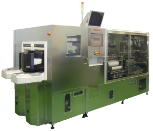
Model:BM-1310W
Achieved stable ball mounting by the AFA original batch transfer method